Math Is Fun Forum
You are not logged in.
- Topics: Active | Unanswered
#1 Re: Jai Ganesh's Puzzles » Oral puzzles » 2026-05-14 22:07:18
Hi,
#6390.
#2 Re: Jai Ganesh's Puzzles » 10 second questions » 2026-05-14 21:29:06
Hi,
#9897.
#3 Re: Exercises » Compute the solution: » 2026-05-14 21:13:13
Hi,
2757.
#4 Re: Exercises » Compute the solution: » 2026-05-10 23:34:52
Hi,
2756.
#6 Re: Exercises » Compute the solution: » 2026-04-18 13:58:13
Correct!
2755.
#7 Re: Exercises » Compute the solution: » 2026-04-14 23:23:53
Hi,
2754.
#8 Re: Exercises » Compute the solution: » 2026-04-14 23:14:39
#9 Re: Exercises » Compute the solution: » 2026-04-14 18:41:57
Check #4.
#10 Re: Exercises » Compute the solution: » 2026-04-13 02:50:27
Hi Rod,
#11 Re: Exercises » Compute the solution: » 2026-04-13 00:45:12
MathsIsFun,
The test message is okay.
Now, it has to run in the forum website.
Sincerely,
Jai.
#12 Re: Exercises » Compute the solution: » 2026-04-10 15:48:13
Hi,
2753.
#13 This is Cool » Slipped Disc » 2026-04-06 23:21:16
- Jai Ganesh
- Replies: 0
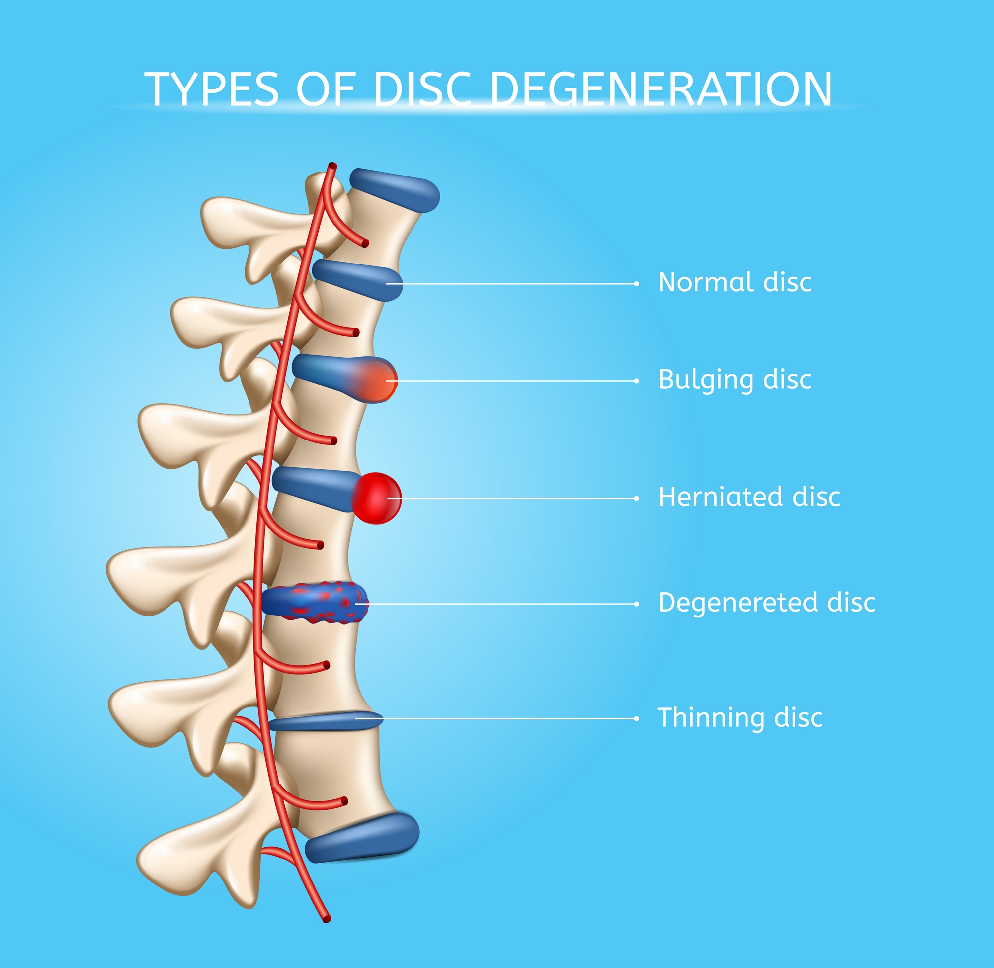
Slipped Disc
Gist
A slipped disc, also called a prolapsed or herniated disc, is when a soft cushion of tissue between the bones in your spine bulges outwards. It's painful if it presses on nerves. It usually gets better slowly with rest, gentle exercise and painkillers.
Symptoms of a slipped disc
A slipped disc can cause:
* lower back pain
* numbness or tingling in your shoulders, back, arms, hands, legs or feet
* neck pain
* problems bending or straightening your back
* muscle weakness
* pain in the buttocks, hips or legs if the disc is pressing on the sciatic nerve (sciatica)
Not all slipped discs cause symptoms. Many people will never know they have slipped a disc.
Other causes of back pain
Sometimes back pain may be a result of an injury such as a sprain or strain, but often there's no obvious reason.
Back pain is rarely caused by anything serious.
Summary
A disc herniation or spinal disc herniation is an injury to the intervertebral disc between two vertebrae, usually caused by excessive strain or trauma to the spine. It may result in back pain, pain or sensation in different parts of the body, and physical disability. The most conclusive diagnostic tool for disc herniation is MRI, and treatments may range from painkillers to surgery. Protection from disc herniation is best provided by core strength and an awareness of body mechanics including good posture.
When a tear in the outer, fibrous ring of an intervertebral disc allows the soft, central portion to bulge out beyond the damaged outer rings, the disc is said to be herniated.
Disc herniation is frequently associated with age-related degeneration of the outer ring, known as the annulus fibrosus, but is normally triggered by trauma or straining by lifting or twisting. Tears are almost always posterolateral (on the back sides) owing to relative narrowness of the posterior longitudinal ligament relative to the anterior longitudinal ligament. A tear in the disc ring may result in the release of chemicals causing inflammation, which can result in severe pain even in the absence of nerve root compression.
Disc herniation is normally a further development of a previously existing disc protrusion, in which the outermost layers of the annulus fibrosus are still intact, but can bulge when the disc is under pressure. In contrast to a herniation, none of the central portion escapes beyond the outer layers. Most minor herniations heal within several weeks. Anti-inflammatory treatments for pain associated with disc herniation, protrusion, bulge, or disc tear are generally effective. Severe herniations may not heal of their own accord and may require surgery.
The condition may be referred to as a slipped disc, but this term is not accurate as the spinal discs are firmly attached between the vertebrae and cannot "slip" out of place.
Details:
Lumbar Disk Disease (Herniated Disk)
What is lumbar disk disease?
The vertebral column, or backbone, is made up of 33 vertebrae that are separated by spongy disks. The spine is divided into 4 areas:
* Cervical spine. The first 7 vertebrae, located in the neck
* Thoracic spine. The next 12 vertebrae, located in the chest area
* Lumbar spine. The next 5 vertebrae, located in the lower back
* Sacral spine. The lowest 5 vertebrae, located below the waist, including the 4 vertebrae that make up the tailbone (coccyx)
The lumbar spine consists of 5 bony segments in the lower back area, which is where lumbar disk disease occurs.
* Bulging disk. With age, the intervertebral disk may lose fluid and become dried out. As this happens, the spongy disk (which is located between the bony parts of the spine and acts as a “shock absorber”) becomes compressed. This may lead to the breakdown of the tough outer ring. This lets the nucleus, or the inside of the ring, bulge out. This is called a bulging disk.
* Ruptured or herniated disk. As the disk continues to break down, or with continued stress on the spine, the inner nucleus pulposus may actually rupture out from the annulus. This is a ruptured, or herniated, disk. The fragments of disk material can then press on the nerve roots located just behind the disk space. This can cause pain, weakness, numbness, or changes in sensation.
Most disk herniations happen in the lower lumbar spine, especially between the fourth and fifth lumbar vertebrae and between the fifth lumbar vertebra and the first sacral vertebra (the L4-L5 and L5-S1 levels).
What causes lumbar disk disease?
Lumbar disk disease is caused by a change in the structure of the normal disk. Most of the time, disk disease happens as a result of aging and the normal breakdown that occurs within the disk. Sometimes, severe injury can cause a normal disk to herniate. Injury may also cause an already herniated disk to worsen.
Who is at risk for lumbar disk disease?
Although age is the most common risk, physical inactivity can cause weak back and abdominal muscles, which may not support the spine properly. Back injuries also increase when people who are normally not physically active participate in overly strenuous activities. Jobs that require heavy lifting and twisting of the spine can also cause back injuries.
What are the symptoms of lumbar disk disease?
The symptoms of lumbar disk disease vary depending on where the disk has herniated and what nerve root it is pushing on. These are the most common symptoms of lumbar disk disease:
* Intermittent or continuous back pain. This may be made worse by movement, coughing, sneezing, or standing for long periods of time.
* Spasm of the back muscles
* Sciatica. This is pain that starts near the back or buttock and travels down the leg to the calf or into the foot.
* Muscle weakness in the legs
* Numbness in the leg or foot
* Decreased reflexes at the knee or ankle
* Changes in bladder or bowel function
The symptoms of lumbar disk disease may look like other health conditions. Always see your healthcare provider for a diagnosis.
How is lumbar disk disease diagnosed?
In addition to a complete medical history and physical exam, you may have one or more of the following tests:
* X-ray. This test uses invisible electromagnetic energy beams to produce images of internal tissues, bones, and organs onto film.
* MRI. This procedure uses a combination of large magnets, radiofrequencies, and a computer to produce detailed images of organs and structures within the body without the use of X-rays.
* Myelogram. This procedure uses dye injected into the spinal canal to make the structure clearly visible on X-rays.
* CT scan. This imaging procedure uses X-rays and computer technology to make detailed images of any part of the body, including the bones, muscles, fat, and organs. CT scans are more detailed than general X-rays.
* Electromyography (EMG). This test measures muscle response or electrical activity in response to a nerve’s stimulation of the muscle. This tests to see if there is any associated nerve damage.
* Discogram. This procedure uses a needle that is inserted into the disk under X-ray guidance.
How is lumbar disk disease treated?
Typically, conservative therapy is the first line of treatment to manage lumbar disk disease. This may include a mix of the following:
* Bed rest
* Education on proper body mechanics (to help decrease the chance of worsening pain or damage to the disk)
* Physical therapy, which may include ultrasound, massage, conditioning, and exercise programs
* Weight control
* Use of a lumbosacral back support
* Medicine to control pain and relax muscles
If these measures fail, you may need surgery to remove the herniated disk. Surgery is done under general anesthesia. Your surgeon will make an incision in your lower back over the area where the disk is herniated. Some bone from the back of the spine may be removed to gain access to the disk. Your surgeon will remove the herniated part of the disk and any extra loose pieces from the disk space.
After surgery, you may be restricted from activity for several weeks while you heal to prevent another disk herniation. Your surgeon will discuss any restrictions with you.
What are possible complications of lumbar disk disease?
Lumbar disk disease can cause back and leg pain that interferes with daily activities. It can lead to leg weakness or numbness and trouble with bowel and bladder control.
What can I do to prevent lumbar disk disease?
Maintaining a healthy weight, participating in regular exercise, and using good posture can lessen your risk for lumbar disk disease. Smoking increases the risk for disk herniation and should be stopped.
Living with lumbar disk disease
Conservative therapy requires patience. But sticking with your treatment plan can reduce back pain and minimize the chance of worsening pain or damage to the disk. Conservative measures and surgery can both take time to be effective.
When should I call my healthcare provider?
Call your healthcare provider right away if your pain increases or if you start having trouble with bowel or bladder control.
Key points about lumbar disk disease
* Lumbar disk disease may occur when a disk in the low back area of the spine bulges or herniates from between the bony area of the spine.
* Lumbar disk disease causes lower back pain and leg pain and weakness that is made worse by movement and activity.
* The first step in treatment is to reduce pain and reduce the risk of further injury to the spine.
* Surgery may be considered if the more conservative therapy fails.
Additional Information
A herniated disc (slipped or ruptured disc) occurs when the soft center of a spinal disc pushes through its outer layer, irritating nearby nerves. Common symptoms include sharp pain in the back, neck, or legs, along with numbness and weakness. Recovery usually takes four to six weeks with conservative treatments like medication, physiotherapy, and movement.
Key Aspects of a Herniated Disc:
* Symptoms: Intense pain (often on one side), pain shooting down the arms or legs (sciatica), numbness, tingling, and muscle weakness.
* Causes: Occurs when discs lose moisture with age, or due to injuries from improper lifting, sudden strains, or chronic strain.
* Risk Factors: Obesity, smoking, and jobs requiring heavy lifting or prolonged sitting.
* Treatment Options: Most cases resolve with non-surgical care, including:
* Pain management: Non-steroidal anti-inflammatory drugs (NSAIDs) like ibuprofen.
* Physical therapy: Exercises to strengthen the back.
* Activity: Remaining active rather than strict bed rest.
* Injections: Cortisone injections for severe inflammation.
* Surgery: Microdiscectomy (if symptoms persist over 6 weeks).
* Recovery Time: Symptoms often improve significantly within 4–6 weeks.
#14 Science HQ » Otoscope » 2026-04-06 22:33:24
- Jai Ganesh
- Replies: 0
Otoscope
Gist
An otoscope is a handheld medical device used to examine the ear canal and eardrum (tympanic membrane) for signs of infection, disease, or injury. It utilizes a light source and magnifying lens to help diagnose conditions like earaches, hearing loss, or wax buildup, and is also used to check the nose and throat.
An otoscope or auriscope is a medical device used by healthcare professionals to examine the ear canal and eardrum. This may be done as part of routine physical examinations, or for evaluating specific ear complaints, such as earaches, sense of fullness in the ear, or hearing loss.
Summary
An ear examination is a normal part of most routine physical examinations by a doctor or nurse. It is also done when an ear infection or other type of ear problem is suspected. An otoscope allows the doctor to look into the ear canal to see the ear drum. Redness or fluid in the eardrum can indicate an ear infection. Some otoscopes (called pneumatic otoscopes) can deliver a small puff of air to the eardrum to see if the eardrum will vibrate (which is normal). An ear examination with an otoscope can also detect a build-up of wax in the ear canal or a rupture or puncture of the eardrum.
Description
An ear examination with an otoscope is usually done by a doctor or a nurse as part of a complete physical examination. The ears may also be examined if an ear infection is suspected due to fever , ear pain , or hearing loss. The child will often be asked to tip the head slightly toward the shoulder opposite of the ear being examined, so the ear to be examined is pointing up. The doctor or nurse may hold the ear lobe as the speculum is inserted into the ear and may adjust the position of the otoscope to get a better view of the ear canal and eardrum. Both ears are usually examined, even if there seems to be a problem with just one ear.
The ear canal is normally skin-colored and is covered with tiny hairs. It is normal for the ear canal to have some yellowish-brown earwax. The eardrum is typically thin, shiny, and pearly-white to light gray in color. The tiny bones in the middle ear can be seen pushing on the eardrum membrane like tent poles. The light from the otoscope will reflect off of the surface of the ear drum.
An ear infection will cause the eardrum to look red and swollen. In cases where the eardrum has ruptured, there may be fluid draining from the middle ear. A doctor may also see scarring, retraction of the eardrum, or bulging of the eardrum.
Details
An otoscope or auriscope is a medical device used by healthcare professionals to examine the ear canal and eardrum. This may be done as part of routine physical examinations, or for evaluating specific ear complaints, such as earaches, sense of fullness in the ear, or hearing loss.
Usage:
Function
An otoscope enables viewing and examination of the ear canal and tympanic membrane (eardrum). As the eardrum is the border between the external ear canal and the middle ear, its characteristics can indicate various diseases of the middle ear space. Otoscopic examination can help diagnose conditions such as acute otitis media (infection of the middle ear), otitis externa (infection of the outer ear), traumatic perforation of the eardrum, and cholesteatoma.
The presence of cerumen (earwax), shed skin, pus, canal skin edema, foreign bodies, and various ear diseases, can obscure the view of the eardrum and thus compromise the value of otoscopy done with a common otoscope, but can confirm the presence of obstructing symptoms.
Otoscopes can also be used to examine patients' noses (avoiding the need for a separate nasal speculum) and upper throats (by removing the speculum).
Method of use
The most common otoscopes consist of a handle and a head. The head contains a light source and a magnifying lens, typically around 8 diopters (3× magnification), to help illuminate and enlarge ear structures. The distal (front) end of the otoscope has an attachment for disposable plastic ear specula.
The examiner first pulls on the pinna (usually the earlobe, side or top) to straighten the ear canal, and then inserts the ear speculum side of the otoscope into the outer ear. It is important to brace the index or little finger of the hand holding the otoscope against the patient's head to avoid injuring the ear canal. The examiner then looks through the lens on the rear of the instrument to see inside the ear canal.
In many models, the examiner can remove the lens and insert instruments like specialized suction tips through the otoscope into the ear canal, such as for removing earwax. Most models also have an insertion point for a bulb that pushes air through the speculum (pneumatic otoscopy) for testing eardrum mobility.
Types
Many otoscopes for doctors' offices are wall-mounted, with an electrical cord providing power from an electric outlet. Portable otoscopes powered by batteries (usually rechargeable) in the handle are also available.
Otoscopes are often sold with ophthalmoscopes as a diagnostic set.
Monocular and binocular
Most otoscopes used in emergency rooms, pediatric offices, general practice, and by internists are monocular devices. These provide a two-dimensional view of the ear canal and its contents, and usually at least a portion of the eardrum.
Another method of performing otoscopy (visualization of the ear) is by using a binocular (two-eyed) microscope in conjunction with a larger plastic or metal ear speculum, which provides a much larger field of view. The microscope is suspended from a stand, which frees up both of the examiner's hands; the patient is placed in a supine position and their head is tilted, which keeps the head stable and enables better lighting. The binocular view enables depth perception, which makes removal of earwax or other obstructing materials easier and less hazardous. The microscope also has up to 40× magnification, allowing more detailed viewing of the entire ear canal, and of the entire eardrum (unless prevented by edema of the canal skin). Subtle changes in the anatomy can also be more easily detected and interpreted.
Traditionally, binocular microscopes are only used by otolaryngologists (ear, nose, and throat specialists) and otologists (subspecialty ear doctors). Their widespread adoption in general medicine is hindered by cost and lack of familiarity among pediatric and general medicine professors in physician training programs. Studies have shown that reliance on a monocular otoscope to diagnose ear disease results in a more than 50% chance of misdiagnosis, as compared to binocular microscopic otoscopy.
Pneumatic otoscope
The pneumatic otoscope is used to examine the eardrum for assessing the health of the middle ear. This is done by assessing the eardrum's contour (normal, retracted, full, or bulging), its color (gray, yellow, pink, amber, white, red, or blue), its translucency (translucent, semi-opaque, opaque), and its mobility (normal, increased, decreased, or absent). The pneumatic otoscope is the standard tool used in diagnosing otitis media (infection of the middle ear).
The pneumatic otoscope has a pneumatic (diagnostic) head, which contains a lens, an enclosed light source, and a nipple for attaching a rubber bulb and tubing. By gently squeezing and releasing the bulb in rapid succession, the degree of eardrum mobility in response to positive and negative pressure can be observed. The head is designed so that an airtight chamber is produced when a speculum is attached and fitted snugly into the patient's ear canal. Using a rubber-tipped speculum or adding a small sleeve of rubber tubing at the end of a plastic speculum, can help improve the airtight seal and also help avoid injuring the patient.
By replacing the pneumatic head with a surgical head, the pneumatic otoscope can also be used to clear earwax from the ear canal, and to perform diagnostic tympanocentesis (drainage of fluid from the middle ear) or myringotomy (creation of incision in the eardrum). The surgical head consists of an unenclosed light source and a lens that can swivel over a wide arc.
Additional Information
An otoscope is a medical instrument equipped with a light source and magnifying lens, used to examine the ear canal and tympanic membrane (eardrum) for conditions like infections, wax buildup, or damage. It is vital for diagnosing ear, nose, and throat (ENT) issues, often identifying causes of earaches, fullness, or hearing loss.
* Usage: During an exam, the clinician inserts a speculum into the ear canal, holding the pinna up and back to improve the view.
* Pneumatic Otoscopy: A specific type of otoscope equipped with a rubber bulb, allowing the provider to test for eardrum mobility and check for fluid behind the eardrum, which is standard for diagnosing ear infections.
* Applications: Besides the ear, it is used for checking nasal cavities and throats.
* Common Conditions Detected: It helps identify otitis externa, cerumen impaction (earwax build-up), eardrum perforations, and cholesteatoma.
The device was originally developed in the 17th century by Wilhelm Fabry. Modern variations include video-otoscopes, which provide high-resolution, shareable images for telemedicine and expert review.

#15 Re: Exercises » Compute the solution: » 2026-04-05 23:39:38
Hi,
2752.
#16 Re: This is Cool » Miscellany » 2026-04-05 22:45:52
2537) Canyon
Gist
A canyon is a deep, narrow valley with steep sides, typically carved by river erosion over millions of years. Known for dramatic landscapes like the Grand Canyon or Antelope Canyon, they are often used for hiking and tourism, or in a metaphorical sense, such as "concrete canyons" in cities. Synonyms include gorge, ravine, chasm, and gully.
A canyon (from Spanish cañón; archaic British English spelling: cañon), gorge or chasm, is a deep cleft between escarpments or cliffs resulting from weathering and the erosive activity of a river over geologic time scales.
Summary
A canyon (from Spanish cañón; archaic British English spelling: cañon), gorge or chasm, is a deep cleft between escarpments or cliffs resulting from weathering and the erosive activity of a river over geologic time scales. Rivers have a natural tendency to cut through underlying surfaces, eventually wearing away rock layers as sediments are removed downstream. A river bed will gradually reach a baseline elevation, which is the same elevation as the body of water into which the river drains. The processes of weathering and erosion will form canyons when the river's headwaters and estuary are at significantly different elevations, particularly through regions where softer rock layers are intermingled with harder layers more resistant to weathering.
A canyon may also refer to a rift between two mountain peaks, such as those in ranges including the Rocky Mountains, the Alps, the Himalayas or the Andes. Usually, a river or stream carves out such splits between mountains. Examples of mountain-type canyons are Provo Canyon in Utah or Yosemite Valley in California's Sierra Nevada. Canyons within mountains, or gorges that have an opening on only one side, are called box canyons. Slot canyons are very narrow canyons that often have smooth walls.
Steep-sided valleys in the seabed of the continental slope are referred to as submarine canyons. Unlike canyons on land, submarine canyons are thought to be formed by turbidity currents and landslides.
Details
Bound by cliffs and cut by erosion, canyons are deep, narrow valleys in the Earth's crust that evoke superlatives and a sense of wonder. Layers of rock outline stories of regional geology like the table of contents to a scientific text.
The landforms commonly break parched terrain where rivers are the major force that sculpts the land. They are also found on ocean floors where the currents dig underwater grooves.
"Grand" is the word used to describe one of the most famous canyons of all. Cut by the Colorado River over the last few million years, the Grand Canyon is 277 miles (446 kilometers) long, more than 5,000 feet (1,500 meters) deep, but only 18 miles (29 kilometers) across at its widest yawn.
Layers of rock in the Grand Canyon tell much about the Colorado Plateau's formative years: a mountain range built with two-billion-year-old rock and then eroded away; sediments deposited from an ancient sea; more mountains; more erosion; another sea; a burst of volcanic activity; and the birth of a river that has since carved the chasm by washing the layers away.
Each layer erodes differently. Some crumble into slopes, others sheer cliffs. They stack together like a leaning staircase that leads to the river's edge. A mixture of minerals gives each layer a distinctive hue of yellow, green, or red.
And its immense size has been seen by very few. More people have orbited the Earth than have hked the Grand Canyon from end to end. Follow the trek of Pete McBride and Kevin Fedarko using this interactive map.
Types of Canyons
Other canyons start where a spring sprouts from the base of a cliff. Such cliffs are composed of permeable, or porous, rock. Instead of flowing off the cliff, water seeps down into the rock until it hits an impermeable layer beneath and is forced to leak sideways. Where the water emerges, the cliff wall is weakened and eventually collapses. A box canyon forms as sections of wall collapse further and further back into the land. The heads of these canyons are marked by cliffs on at least three sides.
Slot canyons are narrow corridors sliced into eroding plateaus by periodic bursts of rushing water. Some measure less than a few feet across but drop several hundred feet to the floor.
Submarine canyons are similar to those on land in shape and form, but are cut by currents on the ocean floor. Many are the mere extension of a river canyon as it dumps into the ocean and flows across the continental shelf. Others are gouged from turbid currents that occasionally plunge to the ocean floor.
Additional Information
A canyon is a deep, narrow valley with steep sides. “Canyon” comes from the Spanish word cañon, which means “tube” or “pipe.” The term “gorge” is often used to mean “canyon,” but a gorge is almost always steeper and narrower than a canyon.
The movement of rivers, the processes of weathering and erosion, and tectonic activity create canyons.
River Canyons
The most familiar type of canyon is probably the river canyon. The water pressure of a river can cut deep into a riverbed. Sediments from the riverbed are carried downstream, creating a deep, narrow channel.
Rivers that lie at the bottom of deep canyons are known as entrenched rivers. They are entrenched because, unlike rivers in wide, flat floodplains, they do not meander and change their course.
The Yarlung Zangbo Grand Canyon in Tibet, a region of southwestern China, was formed over millions of years by the Yarlung Zangbo River. This canyon is the deepest in the world—at some points extending more than 5,300 meters (17,490 feet) from top to bottom. Yarlung Zangbo Canyon is also one of the world’s longest canyons, at about 500 kilometers (310 miles).
Weathering and Erosion
Weathering and erosion also contribute to the formation of canyons. In winter, water seeps into cracks in the rock. This water freezes. As water freezes, it expands and turns into ice. Ice forces the cracks to become larger and larger, eroding bits of stone in the process. During brief, heavy rains, water rushes down the cracks, eroding even more rocks and stone. As more rocks crumble and fall, the canyon grows wider at the top than at the bottom.
When this process happens in soft rock, such as sandstone, it can lead to the development of slot canyons. Slot canyons are very narrow and deep. Sometimes, a slot canyon can be less than a meter (three feet) wide, but hundreds of meters deep. Slot canyons can be dangerous. Their sides are usually very smooth and difficult to climb.
Some canyons with hard, underlying rock may develop cliffs and ledges after their softer, surface rock erodes. These ledges look like giant steps.
Sometimes, entire civilizations can develop on and around these canyon ledges. Native American nations, such as the Hopi and Sinagua, made cliff dwellings. Cliff dwellings were apartment-style shelters that housed hundreds of people. The shaded, elevated ledges in Walnut Canyon and Canyon de Chelly, in Arizona, U.S.A., provided protection from hostile neighbors and the burning desert sun.
Hard-rock canyons that are open at one end are called box canyons. The Hopi and Navajo people often used box canyons as natural corrals for sheep and cattle. They simply built a gate on the open side of the box canyon, and closed it when the animals were inside.
Limestone is a type of hard rock often found in canyons. Sometimes, limestone erodes and forms caves beneath the earth. As the ceilings of these caves collapse, canyons form. The Yorkshire Dales, an area in northern England, is a collection of river valleys and canyons created by limestone cave collapses.
Tectonic Uplift
Canyons are also formed by tectonic activity. As tectonic plates beneath Earth’s crust shift and collide, their movement can change the area’s landscape. Sometimes, tectonic activity causes an area of Earth’s crust to rise higher than the surrounding land. This process is called tectonic uplift. Tectonic uplift can create plateaus and mountains. Rivers and glaciers that cut through these elevated areas of land create deep canyons.
The Grand Canyon, in Arizona, is a product of tectonic uplift. The Grand Canyon, up to 447 kilometers (277 miles) long, 29 kilometers (18 miles) wide, and 1.8 kilometers (6,000 feet) deep, is the largest canyon in the United States. The Grand Canyon has been carved, over millions of years, as the Colorado River cuts through the Colorado Plateau. The Colorado Plateau is a large area that was elevated through tectonic uplift millions of years ago. Geologists debate the age of the canyon itself—it may be between five million and 70 million years old.
Canyons Reveal Earth’s History
Canyons are like silent journals of an area’s history over thousands or even millions of years. By studying the exposed layers of rock in a canyon wall, experts can learn about how the climate changed, what kind of organisms were alive at certain times, and perhaps even how the canyon may change in the future.
For example, geologists studying layers of rock in the Columbia River Gorge, in the U.S. states of Washington and Oregon, discovered that the oldest rocks there are at least 17 million years old. They also found out the rocks are dark-black basalt, made from hardened lava. From this, geologists determined that the rocks formed when volcanoes erupted and their lava spilled out onto the land. Over millions of years, the Columbia River and Ice Age glaciers cut through the area and exposed its volcanic beginnings.
Canyons are also important to paleontology, or the study of fossils. Fossils are often best preserved in dry, hot areas. Since canyons usually form under the same conditions, they are good places to examine fossils.
The layers of sediment revealed by a canyon can make it easier to date fossils. For example, a new area of dinosaur tracks was discovered in the U.S. state of Utah at Glen Canyon National Recreation Area in 2009. These tracks reveal new information about a group of dinosaurs called ornithopods. Paleontologists analyzed the layers of rock surrounding the fossils to estimate how old they were. These new dinosaur tracks show that ornithopods were alive 20 million years earlier than scientists thought.
Geologists study canyons to determine how the landscape will change in the future. The erosion patterns and thickness of different layers can reveal the climate during different years. A series of very dry years will have very thin layers of rock, when little erosion took place. The overall pattern of erosion and layering reveals the rate of water flow, from both the river and rain, through a canyon.
Geologists estimate that the Grand Canyon, for example, is being eroded at a rate of 0.3 meters (one foot) every 200 years. The Colorado Plateau, the geologic area where the Grand Canyon is located, is a very stable area. Geologists expect the Grand Canyon to continue to deepen as long as the Colorado River flows.
Submarine Canyons
Some of the deepest canyons lie beneath the ocean. These submarine canyons cut into continental shelves and continental slopes—the edges of continents that are underwater.
Some submarine canyons were carved by rivers that flowed during periods when the sea level was lower, and the continental shelves were exposed. The Hudson Canyon extends 750 kilometers (450 miles) into the Atlantic Ocean, from the mouth of the Hudson River, in the U.S. states of New York and New Jersey. At least part of the Hudson Canyon was the riverbed during the last ice age, when sea levels were much lower.
Submarine canyons can also develop when powerful ocean currents sweep away sediments. Just as rivers erode land, these currents carve deep canyons in the ocean floor. Strong currents of the Atlantic Ocean prevent Whittard Canyon, about 400 kilometers (248 miles) south of the coast of Ireland, from filling with sediment. Scientists studying Whittard Canyon believe glacial water mixed with seawater to rush into the submarine canyon thousands of years ago.
The formation of some submarine canyons is still a mystery. Monterey Canyon is a deep submarine canyon off the coast of the U.S. state of California. It has been compared to the Grand Canyon because of its size. It is 152 kilometers (95 miles) long and 3.2 kilometers (two miles) deep at its deepest point. Geologists still aren’t certain how Monterey Canyon was formed. One theory is that the canyon was formed by an ancient outlet of the Sacramento or Colorado Rivers. Another theory is that it was formed by tectonic activity—an earthquake splitting apart the rock with enormous force. Scientists believe the canyon was formed 25 million to 30 million years ago.
The depth of submarine canyons makes them hard to explore. Scientists usually use remotely operated vehicles (ROVs) to conduct studies. Sometimes, they can use a submersible, a special kind of submarine. The Monterey Bay Aquarium Research Institute (MBARI) uses a vehicle called Ventana to explore Monterey Canyon. Through the Ventana and other research vehicles, MBARI scientists have discovered new species of organisms living in the canyon, from tiny sea anemones to giant squid.

#17 This is Cool » Bronchitis » 2026-04-05 22:19:42
- Jai Ganesh
- Replies: 0
Bronchitis
Gist
Bronchitis is inflammation of the large airways in your lungs. The inflammation causes you to cough.
Bronchitis can be acute or chronic. Acute bronchitis is usually caused by a viral infection and goes away by itself. Chronic bronchitis is a type of chronic obstructive pulmonary disease (COPD), a long-term lung condition that is usually related to smoking.
What are the symptoms of acute bronchitis?
Someone with bronchitis will have a cough (either dry or bringing up phlegm). The cough may last for 2 to 3 weeks in people with acute bronchitis.
Other symptoms of bronchitis may include:
* wheezing or feeling short of breath
* chest discomfort or pain (due to frequent coughing)
* a blocked or runny nose
* headache
* fever
* aches and pains
* feeling tired
Summary
Bronchitis is inflammation of the bronchi (large and medium-sized airways) in the lungs that causes coughing. Bronchitis usually begins as an infection in the nose, ears, throat, or sinuses. The infection then makes its way down to the bronchi. Symptoms include coughing up sputum, wheezing, shortness of breath, and chest pain. Bronchitis can be acute or chronic.
Acute bronchitis usually has a cough that lasts around three weeks, and is also known as a chest cold. In more than 90% of cases, the cause is a viral infection. These viruses may be spread through the air when people cough or by direct contact. A small number of cases are caused by a bacterial infection such as Mycoplasma pneumoniae or Bordetella pertussis. Risk factors include exposure to tobacco smoke, dust, and other air pollution. Treatment of acute bronchitis typically involves rest, paracetamol (acetaminophen), and nonsteroidal anti-inflammatory drugs (NSAIDs) to help with the fever.
Chronic bronchitis is defined as a productive cough – one that produces sputum – that lasts for three months or more per year for at least two years. Many people with chronic bronchitis also have chronic obstructive pulmonary disease (COPD). Tobacco smoking is the most common cause, with a number of other factors such as air pollution and genetics playing a smaller role. Treatments include quitting smoking, vaccinations, rehabilitation, and often inhaled bronchodilators and steroids.[13] Some people may benefit from long-term oxygen therapy.
Acute bronchitis is one of the more common diseases. About 5% of adults and 6% of children have at least one episode a year. Acute bronchitis is the most common type of bronchitis. By contrast in the United States, in 2018, 9.3 million people were diagnosed with the less common chronic bronchitis.
Details
Bronchitis is an inflammation of the lining of your bronchial tubes. These tubes carry air to and from your lungs. People who have bronchitis often cough up thickened mucus, which can be discolored. Bronchitis may start suddenly and be short term (acute) or start gradually and become long term (chronic).
Acute bronchitis, which often develops from a cold or other respiratory infection, is very common. Also called a chest cold, acute bronchitis usually improves within a week to 10 days without lasting effects, although the cough may linger for weeks.
Chronic bronchitis, a more serious condition, is a constant irritation or inflammation of the lining of the bronchial tubes, often due to smoking. If you have repeated bouts of bronchitis, you may have chronic bronchitis, which requires medical attention. Chronic bronchitis is one of the conditions included in chronic obstructive pulmonary disease (COPD).
Symptoms
If you have acute bronchitis, you may have cold symptoms, such as:
* Cough
* Production of mucus (sputum), which can be clear, white, yellowish-gray or green in color — rarely, it may be streaked with blood
* Sore throat
* Mild headache and body aches
* Slight fever and chills
* Fatigue
* Chest discomfort
* Shortness of breath and wheezing
While these symptoms usually improve in about a week, you may have a nagging cough that lingers for several weeks.
For chronic bronchitis, signs and symptoms may include:
* Cough
* Production of mucus
* Fatigue
* Chest discomfort
* Shortness of breath
Chronic bronchitis is typically defined as a productive cough that lasts at least three months, with bouts that recur for at least two consecutive years. If you have chronic bronchitis, you're likely to have periods when your cough or other symptoms worsen. It's also possible to have an acute infection on top of chronic bronchitis.
When to see a doctor
Contact your doctor or clinic for advice if your cough:
* Is accompanied by a fever higher than 100.4 F (38 C).
* Produces blood.
* Is associated with serious or worsening shortness of breath or wheezing.
* Includes other serious signs and symptoms, for example, you appear pale and lethargic, have a bluish tinge to your lips and nail beds, or have trouble thinking clearly or concentrating.
* Lasts more than three weeks.
Causes
Acute bronchitis is usually caused by viruses, typically the same viruses that cause colds and flu (influenza). Many different viruses — all of which are very contagious — can cause acute bronchitis. Antibiotics don't kill viruses, so this type of medication isn't useful in most cases of bronchitis.
Viruses spread mainly from person to person by droplets produced when an ill person coughs, sneezes or talks and you inhale the droplets. Viruses may also spread through contact with an infected object. This happens when you touch something with the virus on it and then touch your mouth, eyes or nose.
The most common cause of chronic bronchitis is cigarette smoking. Air pollution and dust or toxic gases in the environment or workplace also can contribute to the condition.
Risk factors
Factors that increase your risk of bronchitis include:
* Cigarette smoke. People who smoke or who live with a smoker are at higher risk of both acute bronchitis and chronic bronchitis.
* Low resistance. This may result from another acute illness, such as a cold, or from a chronic condition that compromises your immune system. Older adults, infants and young children have greater vulnerability to infection.
* Exposure to irritants on the job. Your risk of developing bronchitis is greater if you work around certain lung irritants, such as grains or textiles, or are exposed to chemical fumes.
* Gastric reflux. Repeated bouts of severe heartburn can irritate your throat and make you more prone to developing bronchitis.
Complications
Although a single episode of bronchitis usually isn't cause for concern, it can lead to pneumonia in some people. Repeated bouts of bronchitis, however, may mean that you have chronic obstructive pulmonary disease (COPD).
Prevention
To reduce your risk of bronchitis, follow these tips:
* Get an annual flu shot. Many cases of acute bronchitis result from influenza, a virus. Getting a yearly flu vaccine can help protect you from getting the flu. Also ask your doctor or clinic if you need a vaccination that protects against certain types of pneumonia.
* Wash your hands. To reduce your risk of catching a viral infection, wash your hands frequently and get in the habit of using alcohol-based hand sanitizers. Also, avoid touching your eyes, nose and mouth.
* Avoid close contact with people who have a viral infection. Stay away from people who have the flu or another respiratory illness.
* Avoid cigarette smoke. Cigarette smoke increases your risk of chronic bronchitis.
* Wear appropriate face covering. If you have COPD, consider wearing a face mask at work if you're exposed to dust or fumes. Talk to your employer about the appropriate protection. Wearing a face mask when you're going to be among crowds helps reduce exposure to infections.
Additional Information
Bronchitis is when the airways leading to your lungs (trachea and bronchi) get inflamed and fill with mucus. You get a nagging cough as your body tries to get rid of the mucus. Your cough can last two or more weeks. Acute bronchitis is usually caused by a virus and goes away on its own. Chronic bronchitis never really goes away but can be managed.
Overview:
What is bronchitis?
Bronchitis is an inflammation of the airways leading into your lungs.
When your airways (trachea and bronchi) get irritated, they swell up and fill with mucus, causing you to cough. Your cough can last days to a couple of weeks. It’s the main symptom of bronchitis.
Viruses are the most common cause of acute bronchitis. Smoke and other irritants can cause acute and chronic bronchitis.
What are the types of bronchitis?
When people talk about bronchitis, they usually mean acute bronchitis, a temporary condition that makes you cough. Some people get bronchitis so often that it’s considered chronic bronchitis.
Acute bronchitis
Acute bronchitis is usually caused by a viral infection and goes away on its own in a few weeks. Most people don’t need treatment for acute bronchitis.
Chronic bronchitis
You have chronic bronchitis if you have a cough with mucus most days of the month for three months out of the year. This goes on for at least two years.
If you have chronic bronchitis, you may have chronic obstructive pulmonary disease (COPD). Ask your provider about whether you should get tested for COPD.
Who does bronchitis affect?
Anyone can get bronchitis, but you’re at higher risk if you:
* Smoke or are around someone who does.
* Have asthma, COPD or other breathing conditions.
* Have GERD (chronic acid reflux) (Gastroesophageal reflux disease.)
* Have an autoimmune disorder or other illness that causes inflammation.
* Are around smoke, chemicals or toxins in the air.
How does bronchitis affect my body?
When your airways are irritated, your immune system causes them to swell up and fill with mucus. You cough to try to clear the mucus out. As long as there’s mucus or inflammation in your airways, you’ll keep coughing.
Symptoms and Causes:
What are the symptoms of bronchitis?
A persistent cough that lasts one to three weeks is the main symptom of bronchitis. You usually bring up mucus when you cough with bronchitis, but you might get a dry cough instead. You might also hear a whistling or rattling sound when you breathe (wheezing).
You might have other symptoms, including:
* Shortness of breath (dyspnea).
* Fever.
* Runny nose.
* Tiredness (fatigue).
What causes bronchitis?
You almost always get bronchitis from a virus. However, nearly anything that irritates your airways can cause it. Infectious and noninfectious causes of bronchitis include:
* Viruses. Viruses that cause bronchitis include influenza (the flu), respiratory syncytial virus (RSV), adenovirus, rhinovirus (the common cold) and coronavirus.
* Bacteria. Bacteria that cause bronchitis include Bordetella pertussis, Mycoplasma pneumonia and Chlamydia pneumonia.
* Toxins in the air.
* Smoking cigarettes or marijuana (cannabis).
How do you get bronchitis?
You get bronchitis when your airways swell up and fill with mucus. You can get the viruses and bacteria that cause bronchitis from close contact (shaking hands, hugging, touching the same surfaces) with someone who has them. You don’t have to have bronchitis yourself to pass on a virus to someone else who ends up with bronchitis.
Other irritants are in the air you breathe.
Is bronchitis contagious?
Bronchitis itself — inflammation of your airways — isn’t contagious, but the viruses and bacteria that can cause it are. For instance, if you’re sick with the flu, you might get bronchitis too. But when your friend gets the flu from you, their airways don’t get inflamed like yours did.
Is bronchitis a side effect of COVID-19?
You can get bronchitis with almost any virus, including SARS-CoV2, the virus that causes COVID-19. The symptoms of bronchitis can be similar to COVID-19, so make sure you get tested to know which one you have. There haven’t been any studies that show that COVID-19 is any more likely to cause bronchitis than other viral illnesses.
Diagnosis and Tests:
How is bronchitis diagnosed?
Your healthcare provider can tell if you have bronchitis based on your health history and symptoms (clinical diagnosis). They’ll listen to your lungs for signs of congestion and to make sure you’re breathing well. They might test you for viral infections, like the flu or COVID-19.
What tests will be done to diagnose this condition?
There aren’t any specific tests to diagnose bronchitis, but you might be tested for other conditions. Possible tests include:
* Nasal swab. Your healthcare provider may use a soft-tipped stick (swab) in your nose to test for viruses, like COVID-19 or the flu.
* Chest X-ray. If your cough lasts for a long time, you may get a chest X-ray to rule out more serious conditions. Your healthcare provider will use a machine to get pictures of your heart and lungs. They’ll look for signs of other diseases that could cause your symptoms.
* Blood tests. Your provider may do blood tests, using a needle in your arm, to look for infections or check your overall health.
* Sputum test. Your provider may have you cough and then spit into a tube. Your sample will be tested for signs of a virus or bacteria.
* Pulmonary function tests. If your provider thinks you have chronic bronchitis, they may use a machine to test how well your lungs work.

#18 Re: Exercises » Compute the solution: » 2026-04-05 21:33:05
Your solution is right!
#19 Science HQ » Robotics » 2026-04-05 21:21:59
- Jai Ganesh
- Replies: 0
Robotics
Gist
Robotics is the interdisciplinary field of engineering and computer science dedicated to the design, construction, and operation of automated machines (robots) that replicate or enhance human actions. Using sensors and AI, robots perform tasks ranging from repetitive industrial manufacturing to hazardous exploration.
Robotics is a branch of engineering and computer science that involves the conception, design, manufacture and operation of robots. The objective of the robotics field is to create intelligent machines that can assist humans in a variety of ways.
Summary
Robotics is the interdisciplinary study and practice of the design, construction, operation, and use of robots. A roboticist is someone who specializes in robotics. Robotics usually combines four aspects of design work: a power source (e.g. a battery), mechanical construction, a control system (electrical circuits), and software (run by remote control or artificial intelligence).
The goal of most robotics is to design machines that can assist humans in various fields, such as agriculture, construction, domestic work, food processing, inventory management, manufacturing, medicine, military, mining, space exploration, and transportation.
Robots impact humans by displacing workers. Some expect this to occur at an increasing rate, leading to proposed solutions such as basic income. Robotics is itself a lucrative business that creates careers, especially for postgraduates. Roboticists often aim to create machines that seem to interface naturally with humans. The field is under active research and development, with areas of interest including robot kinematics and quantum robotics.
Details
What is Robotics?
Robotics combines computer science, engineering, and technology to design, construct, and utilize machines that are programmed to replicate or substitute human actions and decision-making. These machines, known as robots, are deployed across a broad spectrum of industries to improve productivity, efficiency, and safety. Because robots can be used in so many ways, robotics is a broad, interdisciplinary field, meaning that there are many ways to study it and find a specialized career.
Robots aren't new. They've been around since ancient times, but the Industrial Revolution's rise in manufacturing highlighted the need for widespread automation. The first autonomous machines were built in the mid-20th century. In the 1990s, researchers developed the foundational elements for social robots that could understand and interpret human language and emotion. The advent of artificial intelligence (AI) and machine learning launched the field forward, expanding what is possible for robot automation and autonomy.
Each robot, regardless of its level of autonomy—meaning its ability to operate and make decisions without human supervision or intervention—consists of the same three components: mechanical construction, electrical power and control, and software or programming.
Robotics professionals can design and construct entire robots holistically, or they might focus on one component. They can specialize even further into sensors, control systems, human-robot interaction, and more. With a wide range of ever-growing industry applications, possibilities in the field of robotics are boundless.
What Are Robotics Applications?
Robotics got its start by providing an advantage in manufacturing and industrialization. But now, nearly every industry has found a need for robotic applications to make work more efficient and safe.
Manufacturing
From automobiles to smartphones, robotics have revolutionized the manufacturing industry. Industrial robots can assemble products, sort items, and even fix and maintain other machines in a factory or warehouse.
Healthcare
Medical robots transport medical supplies, perform surgery and diagnostics, manage hospital logistics, and dispense medications. As the robotics industry advances, more sophisticated machines are being developed to improve the efficiency of medical professionals and quality of patient care.
Agriculture
Robots help agricultural businesses meet growing global demand by performing routine tasks such as planting, pest and weed management, and harvesting.
Construction
Construction teams are safer, efficient, and more accurate thanks to robotic assistance. Autonomous technologies operate construction machinery and complete specialized tasks like welding, drilling, and brick-laying.
Shipping and Delivery
Robotics have streamlined the logistics of shipping and delivering goods. Autonomous mobile robots maneuver through warehouses and collect items for shipments, while companies deploy delivery bots to complete local deliveries in a timely manner.
More Real-World Robotics
Robots and autonomous technologies keep clean energy affordable through system installation and maintenance. Robots navigate mines for materials and analyze structural integrity. Search and rescue robots help disaster response teams by navigating floodwaters and putting out forest fires. In the home, robots keep surfaces clean and sanitized, mow lawns, engage with children, and assist people with disabilities.
Types of Robots
Robots come in all shapes and sizes, which is understandable given the variety of purposes they serve, from education and entertainment to integration as vital components in the manufacturing industry.
* Humanoid robots look like and mimic human behavior. Development of more advanced models is ongoing, as demand rises for robots to assist with research and professional services.
* Industrial robots are heavy-duty machines that automate manufacturing processes at scale.
* Mobile robots sort and deliver goods in warehouses, in the home, and on the street.
* Collaborative robots, or cobots, work in conjunction with people in the service industry and manufacturing.
* Social robots are AI-powered machines with a variety of applications in education, early childhood development, disability assistance, and companionship.
* Microrobots and nanorobots run diagnostics, monitor and treat diseases, and assess injuries.
What is Robotics?
Robotics combines computer science, engineering, and technology to design, construct, and utilize machines that are programmed to replicate or substitute human actions and decision-making. These machines, known as robots, are deployed across a broad spectrum of industries to improve productivity, efficiency, and safety. Because robots can be used in so many ways, robotics is a broad, interdisciplinary field, meaning that there are many ways to study it and find a specialized career.
Robots aren't new. They've been around since ancient times, but the Industrial Revolution's rise in manufacturing highlighted the need for widespread automation. The first autonomous machines were built in the mid-20th century. In the 1990s, researchers developed the foundational elements for social robots that could understand and interpret human language and emotion. The advent of artificial intelligence (AI) and machine learning launched the field forward, expanding what is possible for robot automation and autonomy.
Each robot, regardless of its level of autonomy—meaning its ability to operate and make decisions without human supervision or intervention—consists of the same three components: mechanical construction, electrical power and control, and software or programming.
Robotics professionals can design and construct entire robots holistically, or they might focus on one component. They can specialize even further into sensors, control systems, human-robot interaction, and more. With a wide range of ever-growing industry applications, possibilities in the field of robotics are boundless.
What Are Robotics Applications?
Robotics got its start by providing an advantage in manufacturing and industrialization. But now, nearly every industry has found a need for robotic applications to make work more efficient and safe.
Manufacturing
From automobiles to smartphones, robotics have revolutionized the manufacturing industry. Industrial robots can assemble products, sort items, and even fix and maintain other machines in a factory or warehouse.
Healthcare
Medical robots transport medical supplies, perform surgery and diagnostics, manage hospital logistics, and dispense medications. As the robotics industry advances, more sophisticated machines are being developed to improve the efficiency of medical professionals and quality of patient care.
Agriculture
Robots help agricultural businesses meet growing global demand by performing routine tasks such as planting, pest and weed management, and harvesting.
Construction
Construction teams are safer, efficient, and more accurate thanks to robotic assistance. Autonomous technologies operate construction machinery and complete specialized tasks like welding, drilling, and brick-laying.
Shipping and Delivery
Robotics have streamlined the logistics of shipping and delivering goods. Autonomous mobile robots maneuver through warehouses and collect items for shipments, while companies deploy delivery bots to complete local deliveries in a timely manner.
More Real-World Robotics
Robots and autonomous technologies keep clean energy affordable through system installation and maintenance. Robots navigate mines for materials and analyze structural integrity. Search and rescue robots help disaster response teams by navigating floodwaters and putting out forest fires. In the home, robots keep surfaces clean and sanitized, mow lawns, engage with children, and assist people with disabilities.
Types of Robots
Robots come in all shapes and sizes, which is understandable given the variety of purposes they serve, from education and entertainment to integration as vital components in the manufacturing industry.
Humanoid robots look like and mimic human behavior. Development of more advanced models is ongoing, as demand rises for robots to assist with research and professional services.
Industrial robots are heavy-duty machines that automate manufacturing processes at scale.
Mobile robots sort and deliver goods in warehouses, in the home, and on the street.
Collaborative robots, or cobots, work in conjunction with people in the service industry and manufacturing.
Social robots are AI-powered machines with a variety of applications in education, early childhood development, disability assistance, and companionship.
Microrobots and nanorobots run diagnostics, monitor and treat diseases, and assess injuries.
Advantages and Disadvantages of Using Robots
Robots have expanded what's possible across industries. But their onset has drawbacks as well as benefits.
Advantages of Robotics
Increased accuracy: Robots perform repetitive tasks with greater precision and accuracy than humans, allowing people to focus on more complex tasks.
Enhanced productivity: Robots can work at a faster pace than humans for longer durations, leading to more consistent and higher-volume productivity.
Improved safety: Robots can complete tasks and operations in unsafe environments, protecting workers from injuries.
Rapid innovation: Robots equipped with advanced sensors and cameras can collect and organize data quickly, leading to faster analysis and innovation.
Greater cost-efficiency: As robots accelerate productivity, they can be a more cost-effective option for companies over human labor.
Disadvantages of Robotics
Workforce displacement: Robotic process automation may put some human employees out of work and change the skills necessary for work in certain sectors.
Limited creativity: Robots aren't good with surprises. In unexpected situations, robots don't possess the same level of problem-solving skills as humans.
Security risks: Robots can be subject to cyber attacks, potentially exposing large amounts of data.
Maintenance costs: Robotic machines are expensive to repair and maintain. Faulty equipment can lead to production disruptions and revenue loss.
Environmental waste: Robot construction requires large amounts of raw materials. Discarded robots and parts can lead to pollution and waste disposal issues.
What Skills Do People In Robotics Fields Need?
Robotics professionals need to possess an interest and understanding of all three robotics components: mechanical construction, electrical power and control, and programming.
While the level of understanding across the three components may vary depending on career or role, all robotics professionals must have strong mathematical skills, expertise in physical sciences, computer programming proficiency, and ample problem-solving abilities. Robotics professionals must also possess strong communication skills in order to work well with others and present their developments to clients and stakeholders. Professionals can specialize based on skill, expertise, and interest.
What Careers Are There in Robotics?
The robotics field is broad and ever-expanding. Robotics jobs and careers vary widely depending on specialization, interest, and industry. Different robotics careers require different kinds of skills and education. Some standard robotics jobs include the following:
* Robotics engineer
* Mechatronics engineer
* Robotics programmer
* Automation engineer
* Robotics integration designer
* Industrial engineer
* Software engineer
* Mechanical engineer
* User interface/user experience (UI/UX) designer
* Robotics operator
* Controls engineer
* Manufacturing technician
The Future of Robotics
The future of robotics relies heavily on the advancements of artificial intelligence (AI). Advanced AI can affect robotic autonomy and problem-solving abilities as autonomous machines develop neural frameworks. Through generative AI tools, robots acquire the capability to adapt to unexpected situations and communicate with human operators more effectively.
As robots become increasingly prevalent in everyday life, the field of human-robot interaction is expanding to understand how people can operate and live harmoniously with robots in homes, in the workplace, and on the street. As interactions between humans and robotic systems grow, the look and behavior of robots has changed to be more visually appealing to humans, better understand human language and emotion, and respond more effectively.
With millions of robots being used around the world, societal and organizational developments will be needed as humans determine how to best work alongside robots and adapt the workforce to counteract the rise in displaced jobs from robotic labor. With the introduction of technologies such as AI and machine learning, humans will need to adapt to work alongside robots in a more efficient and productive society.
Additional Information
Robotics is design, construction, and use of machines (robots) to perform tasks done traditionally by human beings. Robots are widely used in such industries as automobile manufacture to perform simple repetitive tasks, and in industries where work must be performed in environments hazardous to humans. Many aspects of robotics involve artificial intelligence; robots may be equipped with the equivalent of human senses such as vision, touch, and the ability to sense temperature. Some are even capable of simple decision making, and current robotics research is geared toward devising robots with a degree of self-sufficiency that will permit mobility and decision-making in an unstructured environment. Today’s industrial robots do not resemble human beings; a robot in human form is called an android.
Japanese roboticist Masahiro Mori proposed that as human likeness increases in an object’s design, so does one’s affinity for the object, giving rise to the phenomenon called the "uncanny valley." According to this theory, when the artificial likeness nears total accuracy, affinity drops dramatically and is replaced by a feeling of eeriness or uncanniness. Affinity then rises again when true human likeness—resembling a living person—is reached. This sudden decrease and increase caused by the feeling of uncanniness creates a “valley” in the level of affinity.

#20 Re: Jai Ganesh's Puzzles » Oral puzzles » 2026-04-05 17:17:26
Hi,
#6389.
#21 Re: Exercises » Compute the solution: » 2026-04-05 16:25:50
Hi,
2751.
#22 Re: Dark Discussions at Cafe Infinity » crème de la crème » 2026-04-05 00:02:15
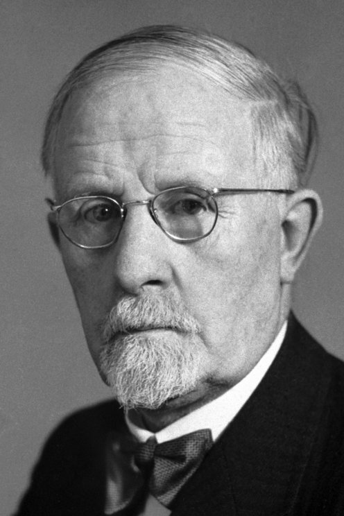
2474) Walter Rudolf Hess
Gist:
Work
The diencephalon of both human and animal brains has cells that govern many behaviors. During the 1930s Walter Hess inserted a narrow metal thread into different parts of anesthetized cats’ hypothalamus, an area on the underside of the diencephalon. When the cats awoke, he could trigger different behaviors with weak electrical impulses to different parts of the hypothalamus—not just simple reactions but complex behaviors. Among other things, the cats could be made to display defensive and aggressive behaviors and to curl up and go to sleep.
Summary
Walter Rudolf Hess (born March 17, 1881, Frauenfeld, Switz.—died Aug. 12, 1973, Ascona) was a Swiss physiologist, who received (with António Egas Moniz) the 1949 Nobel Prize for Physiology or Medicine for discovering the role played by certain parts of the brain in determining and coordinating the functions of internal organs.
Originally an ophthalmologist (1906–12), Hess turned to the study of physiology, becoming a research assistant first at the Physiological Institute at the University of Zürich in 1912 and then at the University of Bonn in 1915. In 1917 he was appointed professor of physiology and later director of the Physiological Institute (1917–51) at Zürich. He became interested in the study of the autonomic nervous system—those nerves originating at the base of the brain and extending throughout the spinal cord that control the automatic functions such as digestion and excretion. They also trigger the activities of a group of organs that respond to complex stimuli, such as stress.
Using fine electrodes to stimulate or destroy specific areas of the brain in freely moving conscious cats, Hess found that the seat of autonomous function lies at the base of the brain, in the medulla oblongata and the diencephalon (interbrain), particularly that part of the interbrain known as the hypothalamus. He mapped the control centres for each function to such a degree that he could induce the physical behaviour pattern of a cat confronted by a dog simply by stimulating the proper points on the animal’s hypothalamus. He also studied the mechanisms of goal-directed movements and established the concept of anticipatory motor control on posture to enable voluntary motor action. Among Hess’s books is The Biology of Mind (1964).
Details
Walter Rudolf Hess (17 March 1881 – 12 August 1973) was a Swiss physiologist who won the Nobel Prize in Physiology or Medicine in 1949 for mapping the areas of the brain involved in the control of internal organs. He shared the prize with Egas Moniz.
Early life and education
Hess was born in Frauenfeld as the second of three children to Clemens Hess and Gertrud Hess (née Fischer). His father encouraged him to pursue a scientific career and with him he conducted experiments in his physics laboratory. He started to study medicine in Lausanne in 1899 and then in Berlin, Kiel and Zürich. He received his medical degree from the University of Zurich in 1906 and trained as surgeon in Münsterlingen (in the same canton as his birthplace Frauenfeld) under Conrad Brunner (1859–1927). He developed a viscosimeter to measure blood viscosity and published his dissertation in 1906 titled Zum Thema Viskosität des Blutes und Herzarbeit. In 1907, he went to the University of Zurich to study under Otto Haab to be trained as an ophthalmologist and opened his own private practice in Rapperswil SG. In these years, he developed the "Hess screen", married Louise Sandmeier and in 1910 their daughter Gertrud Hess was born. In 1913 his son Rudolf Max Hess was born.
In 1912, he left his lucrative private practice as an ophthalmologist and went into research under Justus Gaule (1849–1939), habilitating in 1913 to become Privatdozent. His primary interests were the regulation of blood flow and respiration. During the First World War he spent a year at the Physiological Institute of the University of Bonn under Max Verworn. In 1916, Gaule retired and Hess first became interim director of the Department of the Physiological Institute at the University of Zurich. Hess served as full professor and director of the institute from 1917 until his retirement in 1951.
In the 1930s, he began mapping the parts of the diencephalon that control the internal organs using cats. This research won him the Nobel prize in Physiology and Medicine 1949. Hess also helped to found the meteorological research foundation International Foundation for the High Alpine Research Station Jungfraujoch in 1930 and served as its director until 1937. Furthermore, he politically campaigned against the anti-vivisectionists that wanted to forbid animal experimentation.
Hess retired in 1951 but continued working at the university in an office. In 1967, he moved to Ascona and died of heart failure in 1973 at the age of 92 in Locarno, Switzerland. His widow died in 1987.
Research
Hess used brain stimulation techniques developed in the late 1920s. Using electrodes, Hess stimulated the brain at well-defined anatomical regions. This allowed him to map regions of the brain to specific physiological responses. He developed a special technique he called "interrupted direct-current (DC) stimulation" which used stimuli of long duration (typically 12.5 or 25 ms) with ramp-like upward and downward slopes. Also, the stimuli were rather weak (around 0.5–1.5 V) and of low frequency (2–12 Hz, usually 8 Hz) and he used very fine electrodes with a diameter of 0.25 mm.
By stimulating the hypothalamus, he could induce behaviors from excitement to apathy; depending on the region of stimulation. He found that he could induce different responses when stimulating the anterior (lateral) hypothalamus compared to stimulating the posterior ventromedial hypothalamus. When stimulating the anterior part, he could induce fall of blood pressure, slowing of respiration and responses such as hunger, thirst, micturition (urination) and defecation. Stimulation of the posterior part led to extreme excitement and defense-like behavior.
Hess also found that he could induce sleep in cats – a finding that was highly controversial at the time but later confirmed by other researchers, including his son Rudolf Max Hess.
#23 This is Cool » Angiogram » 2026-04-04 23:00:25
- Jai Ganesh
- Replies: 0
Angiogram
Gist
An angiogram is a scan that shows blood flow through arteries or veins, or through the heart, using X-rays, computed tomography angiography (CTA) or magnetic resonance angiography (MRA). The blood vessels appear on the image after a contrast dye is injected into the blood, which lights up on the scan wherever it flows.
Angiography may be the first step of a procedure to find and fix a blood vessel blockage, aneurysm, structural heart or valve disease.
Summary
An angiogram is a type of X-ray used to examine blood vessels.
Blood vessels don’t show up clearly on ordinary X-rays, so a special dye is injected into the area being examined. The dye highlights the blood vessels as it moves through them. The medical name for this is a catheter angiogram.
Less commonly, angiograms can also be carried out using magnetic resonance imaging(MRI) and computerised tomography (CT) techniques.
Why angiograms are used
An angiogram can help diagnose conditions that affect blood vessels and the flow of blood through them. These include:
* coronary heart disease – the blood flow through the artery that supplies the heart muscle is disrupted because it has become narrowed
* aneurysm – a section of a blood vessel wall bulges outwards due to a weakness in the wall
* atherosclerosis – blood vessels become clogged up with fatty substances, such as cholesterol; an angiogram can be used to assess the level of atherosclerosis in specific blood vessels
Details
An angiogram is a diagnostic procedure that uses imaging to show your provider how your blood flows through your blood vessels or heart. An injected contrast material makes it easy to see where blood is moving and where blockages are. Your provider can use X-rays or other types of imaging for your angiogram.
Cerebral Arteriogram
An arteriogram is an X-ray of the blood vessels. It’s used to look for changes in the blood vessels, such as:
* Ballooning of a blood vessel (aneurysm)
* Narrowing of a blood vessel (stenosis)
* Blockages
This test is also called angiogram.
For arteriogram, your healthcare provider inserts a catheter into a large blood vessel and injects contrast dye. The contrast dye causes the blood vessels to appear on the X-ray image. This lets the healthcare provider better see the vessel(s) under exam.
Many arteries can be seen on an arteriogram, including those of the legs, kidneys, brain, and heart. A cerebral arteriogram is used to look at the blood vessels of the brain, head, or neck.
For a cerebral arteriogram, a catheter is usually inserted into an artery in the groin. Sometimes, an artery in the arm is used. Rarely, an artery in the neck may need to be used. The groin artery is most commonly used because it’s easier to get to. Once the catheter is inserted, the contrast dye is injected. Next, a series of X-rays are made. These images show the arteries, veins, and capillaries and blood flow in the brain.
What is computed tomography (CT) angiography?
CT angiography is a type of medical test that combines a CT scan with an injection of a special dye to produce pictures of blood vessels and tissues in a part of your body. The dye is injected through an intravenous (IV) line placed in your arm or hand.
A computerized tomography scan, or CT scan, is a type of X-ray that uses a computer to make cross-sectional images of your body. The dye injected to perform CT angiography is called a contrast material because it enhances blood vessels and tissues that are being studied.
Why might I need a computed tomography angiography?
* To find or measure the size of an aneurysm (a blood vessel that has become enlarged and may be in danger of rupturing)
* To find blood vessels that have become narrowed by atherosclerosis (fatty material that forms plaques in the walls of arteries)
* To follow vessels involved by dissections, which are tears that can form in the wall of vessels
* To find abnormal blood vessel formations inside your brain
* To identify blood vessels damaged by injury
* To find blood clots that may have formed in your leg veins and traveled into your lungs
* To evaluate a tumor that is fed by blood vessels
Information from CT angiography may help prevent a stroke or a heart attack. This type of test may also help your health care provider plan cancer treatment or prepare you for a kidney transplant. Your health care provider may have other reasons for ordering this test.
What is fluoroscopy?
Fluoroscopy is a study of moving body structures--similar to an X-ray "movie." A continuous X-ray beam is passed through the body part being examined. The beam is transmitted to a TV-like monitor so that the body part and its motion can be seen in detail. Fluoroscopy, as an imaging tool, enables physicians to look at many body systems, including the skeletal, digestive, urinary, respiratory, and reproductive systems.
Fluoroscopy may be performed to evaluate specific areas of the body, including the bones, muscles, and joints, as well as solid organs, such as the heart, lung, or kidneys.
Other related procedures that may be used to diagnose problems of the bones, muscles, or joints include X-rays, myelography ( myelogram ), computed tomography ( CT scan ), magnetic resonance imaging ( MRI ), and arthrography.
What is magnetic resonance angiography?
You’ve probably heard about the test called magnetic resonance imaging or MRI. In this test, radio waves, a magnetic field, and a computer create a scan of your body parts to look for health problems.
Magnetic resonance angiography–also called a magnetic resonance angiogram or MRA–is a type of MRI that looks specifically at the body’s blood vessels. Unlike a traditional angiogram, which requires inserting a catheter into the body, magnetic resonance angiography is a far less invasive and less painful test.
During magnetic resonance angiography, you lie flat inside the magnetic resonance imaging scanner. This is a large, tunnel-like tube. In some cases, a special dye, known as contrast, may be added to your bloodstream to make your blood vessels easier to see. When needed, the contrast is given with an intravenous (IV) needle.
What is a resting radionuclide angiogram?
Resting radionuclide angiogram (RNA) is a type of nuclear medicine test. Doctors use a tiny amount of a radioactive substance, called a tracer, during the scan to help show the heart’s chambers in motion. This test can tell the doctor how well the heart pumps and how much blood is pumped with each heartbeat. This is called the ejection fraction.
Your doctor injects a radioactive tracer (usually technetium) into an arm vein. The tracer “tags" blood cells so your doctor can track them with a scanner as they move through the heart. A special camera (called a gamma camera) then records the heart muscle at work, like a movie. Your doctor can match these recordings with the electrocardiogram (ECG). An ECG is a recording of the heart's electrical activity.
If the heart muscle doesn’t move normally, or not enough blood is pumped out by the heart, it may be a sign of one or more of the following:
* Injury to the heart muscle, possibly as a result of decreased blood flow to heart muscle due to clogged heart arteries
* An enlargement of one or more of the heart's chambers
* Aneurysm (a weak area in the heart muscle)
* Toxic effects of certain medicines
* Heart failure
Additional Information
An angiogram is a diagnostic procedure that uses imaging to show your provider how your blood flows through your blood vessels or heart. An injected contrast material makes it easy to see where blood is moving and where blockages are. Your provider can use X-rays or other types of imaging for your angiogram.
Overview:
An angiogram uses X-ray images and contrast dye to show blockages in blood vessels.
What is an angiogram?
An angiogram is a diagnostic procedure that uses X-ray images to look for blockages or narrow spots in your blood vessels (arteries or veins). An angiogram test can show how blood circulates in blood vessels at specific locations in your body. Healthcare providers use an angiogram of your heart, neck, kidneys, legs or other areas to locate the source of an artery or vein issue.
Your healthcare provider may want to do an angiogram procedure when you have signs of blocked, damaged or abnormal blood vessels. An angiogram test helps your provider determine the source of the problem and the extent of damage to your blood vessels.
With an angiogram procedure, your provider can diagnose and plan treatment for conditions like:
* Coronary artery disease (blockage or narrowing in the arteries that supply your heart)
* Peripheral artery disease (blockage or narrowing in your leg arteries)
* Blood clots (mass of blood cells)
* Aneurysm (weak artery wall)
Test Details:
How does an angiogram work?
An angiogram procedure involves injecting contrast material (dye) that your provider can see with an X-ray machine. Images on a screen show blood flow and blockages in your blood vessels.
Your provider will give you medicine to make sure you’re relaxed and comfortable. Most people receive sedation. Others get general anesthesia, which makes them sleep. Either way, someone will need to drive you home afterward.
How to prepare for an angiogram procedure
Before your angiogram test, your provider may want to check your blood to determine how well your blood clots. They also want to make sure your kidneys are working well.
Medications
Always consult with your provider before you stop taking any medication, especially antiplatelets and anticoagulants. With provider approval:
* Don’t take clopidogrel for five days before your procedure.
* Don’t take blood thinners like dipyridamole or warfarin within 72 hours before the test and 24 hours after the test.
* Take all other medications as usual.
* If you have diabetes, ask your provider for instructions about if and when to take your insulin and/or medicine.
Don’t eat anything after midnight the night before your angiogram. If you’re having general anesthesia during the procedure, don’t eat or drink anything after midnight.
The day of your angiogram
Be sure to:
* Drink only clear liquids for breakfast on the day of your procedure.
* Leave your jewelry and other valuables at home.
* Make sure you arrange for a responsible adult to drive you home.
* Bring a current list of your medications and allergies.
* Bring a book or magazine in case your healthcare provider has to handle an urgent case before yours.
* Let all of your providers know if you have diabetes.
* Change into a hospital gown and lie down on a special X-ray table.
* Meet with your provider to review instructions, questions and your medical history.
What to expect during angiography
During an angiogram procedure, your provider will:
1) Numb the area where the catheter will go.
2) Access your blood vessel with a needle.
3) Thread a wire through the needle.
4) Slide a long, slender tube called a catheter over the needle and into a large artery (usually in your groin or wrist area).
5) Slowly and carefully thread the catheter through your artery until the catheter’s tip reaches the part of the blood vessel they want to examine.
6) Inject a small amount of contrast material (dye) through the catheter and into your blood vessel segment. For a few seconds, this can make you feel flushed or like you need to pee.
7) Take X-rays.
8) Watch where the contrast agent goes on the X-ray monitor to see where and how well blood is moving in your blood vessels.
How long does an angiogram take?
An angiogram can take as little as 15 minutes. But some can take a few hours. It depends on what procedures your provider does after they find the issue.
If your provider finds a blockage, they may treat it right away with an angioplasty. This procedure uses a tiny balloon to force the blockage against your artery wall. An angioplasty may be all you need if it makes your blood flow better and there’s less than 30% of your blockage left after the procedure.
If an angioplasty doesn’t create a large enough opening for blood to get through, you may need a stent. This tiny metal tube stays in your blood vessel to keep it open. Your provider can place this right after your angioplasty.
Another treatment, surgery for your heart (coronary artery bypass) or legs (peripheral artery bypass), creates a way around your blockage. A provider will do this on a different day.
What to expect after angiography
Your healthcare provider will take out the catheter and bandage the area where they punctured your skin. They’ll press on the bandaged area for at least 15 minutes to stop or prevent bleeding.
If they put the catheter in through your leg, you’ll need to rest in bed for four to six hours. This will make your incision less likely to bleed.
Your provider will evaluate you and discuss at-home instructions with you before you go home.
Angiogram recovery
You should be able to go home the same day as your angiogram procedure or the next day, even if you had angioplasty and stenting. Because you received anesthesia, you’ll need someone to drive you home.
After you get home, don’t lift anything heavier than 10 pounds or stoop or bend for the next two days. This should keep your incision from bleeding.
A responsible adult should stay with you overnight after your procedure. Some people may need to spend the night in the hospital for their angiogram recovery.
If you have diabetes, don’t take metformin for 48 hours after the test. This reduces the risk of kidney complications.
Drinking water will help flush the contrast dye out of your system.
What are the risks of angiography?
Angiogram risks are low. But you can have complications in the area where your provider went through your skin to reach your artery. Angiogram complications happen in less than 1% of cases.
Risks of an angiogram procedure usually involve your puncture site and include:
* Bruises, which are common and go away in one to three weeks
* Bleeding
* Infection
* Pain
* Kidney issues
* An allergic reaction to the contrast material (dye)
* Injury to blood vessels
* Abnormal heart rhythm (arrhythmia) or cardiac arrest that requires resuscitation
* A blood vessel blockage from a blood clot that could cause a heart attack or stroke (rarely)
* A blood vessel leak (rarely).

#24 Science HQ » Ulcer » 2026-04-04 19:16:56
- Jai Ganesh
- Replies: 0
Ulcer
Gist
The most common causes of peptic ulcers are Helicobacter pylori (H. pylori) infection and nonsteroidal anti-inflammatory drugs (NSAIDs). Other causes of peptic ulcers are uncommon or rare. People with certain risk factors are more likely to develop ulcers.
Mouth ulcers typically heal on their own within 1 to 2 weeks, though larger ones can last up to 6 weeks. Stomach ulcers usually heal within 4 to 8 weeks with proper treatment, though severe cases may take over 12 weeks. See a doctor if mouth ulcers last over 3 weeks.
Summary:
What is an ulcer?
Ulcers are sores on the lining of your stomach or small intestine. Sores also could be on your esophagus (throat). Most ulcers are located in the small intestine. These ulcers are called duodenal ulcers. Stomach ulcers are called gastric ulcers. Ulcers in the throat are called esophageal ulcers.
Ulcer symptoms:
Common ulcer symptoms
* Discomfort between meals or during the night (duodenal ulcer)
* Discomfort when you eat or drink (gastric ulcer)
* Stomach pain that wakes you up at night
* Feel full fast
* Bloating, burning, or dull pain in your stomach
* Comes and goes days or weeks at a time
* The discomfort lasts for minutes or hour
Bleeding ulcer symptoms
If your ulcer becomes perforated (torn), it becomes a bleeding ulcer. This can cause the following symptoms:
* Nausea
* Vomiting blood
* Unexpected weight loss
* Blood in your stool or dark stools
* Pain in your back
What causes ulcers?
A bacterial infection called Heliocobacter pylori (H. pylori) is typcially what causes ulcers. Acids from the foods we eat can make the pain and discomfort worse. Long-term use of aspirin or anti-inflammatory medicines (ibuprofen) are also a common cause of ulcers. Stress and spicy foods can make an ulcer worse.
How is an ulcer diagnosed?
Your doctor will ask you about your symptoms. They may do an endoscopy. This procedure involves inserting a thin, flexible tube attached to a camera down your throat and into your stomach. Your doctor will test your blood, breath, or stool for H. pylori. They also can test a sample of your stomach lining. Your doctor also will ask you if you regularly take aspirin or anti-inflammatory medicines.
Details:
What Are Stomach Ulcers?
Stomach ulcers, also known as peptic ulcers, are open sores in the lining of your stomach or the upper part of your small intestine. The ulcer forms when stomach acid eats away at the mucus that protects the lining of your digestive tract.
Types of peptic ulcers
Gastric ulcer: It occurs when a sore forms in the lining of your stomach.
Duodenal ulcer: This happens when a sore develops in the upper part of your intestine.
Esophageal ulcer: This is when a sore forms in the lining of your esophagus, which is the tube that carries food and liquid from your throat to your stomach.
Causes of Stomach Ulcers
Until the mid-1980s, the conventional wisdom was that ulcers form as a result of stress, being prone to excessive stomach acid secretion because of genetics, and poor lifestyle habits (including overindulging in rich and fatty foods, alcohol, caffeine, and tobacco). It was believed that such factors could lead to a buildup of stomach acids that could erode the protective lining of the stomach, duodenum, or esophagus.
While too much stomach acid secretion certainly plays a role in the development of ulcers, a relatively recent theory holds that bacterial infection is the primary cause of peptic ulcers. Research since the mid-1980s has shown that the bacterium Helicobacter pylori(H. pylori) is present in more than 90% of duodenal ulcers and about 80% of stomach ulcers. However, more recent figures indicate those percentages are declining.
Most people infected with H. pylori do not get ulcers. But in others, it can raise the amount of acid, break down the protective mucus layer, and irritate the digestive tract. Experts aren’t sure how an H. pylori infection spreads. They think it may pass from person to person through close contact, such as kissing. You may also get it from unclean food and water.
Other factors also seem to contribute to ulcer formation, especially in someone with an H. pylori infection, including:
* Overuse of over-the-counter painkillers (such as aspirin, ibuprofen, and naproxen). If you’ve been taking aspirin often and for a long time, you’re more likely to get a peptic ulcer. The same is true for other nonsteroidal anti-inflammatory drugs (NSAIDs). They include ibuprofen and naproxen. NSAIDs block your body from making a chemical that helps protect the inner walls of your stomach and small intestine from stomach acid. Other types of pain meds, such as acetaminophen, won’t lead to peptic ulcers.
* Heavy alcohol use
* Psychological stress
* Smoking
Your risk for peptic ulcers also increases if you:
* Use steroids and have high calcium levels. If you use steroids often and have high levels of calcium in your blood, known as hypercalcemia, you can be more prone to ulcers.
* Are older. Studies show that stomach ulcers are more likely to develop in older people. This may be because arthritis is prevalent in older people, and easing arthritis pain can mean taking daily doses of aspirin or ibuprofen. Also, with advancing age, the pylorus (the valve between the stomach and duodenum) relaxes and allows extra bile (a compound produced in the liver to aid in digestion) to seep up into the stomach and erode the stomach lining.
* Have type A blood. For an unknown reason, people with type A blood are more likely to develop cancerous stomach ulcers.
* Have type O blood. Duodenal ulcers tend to appear in people with type O blood, possibly because they do not produce the substance on the surface of blood cells that may protect the lining of the duodenum.
* Have Zollinger-Ellison syndrome. If you have Zollinger-Ellison syndrome, which is a rare condition where tumors in your pancreas or duodenum (called gastrinomas) cause your stomach to make too much acid, you are at a greater risk of developing peptic ulcers.
Additional Information:
Definition
A peptic ulcer is an open sore or raw area in the lining of the stomach (gastric ulcer) or in the first part of the small intestine (duodenal ulcer).
There are two types of peptic ulcers:
Gastric ulcer -- occurs in the stomach
Duodenal ulcer -- occurs in the first part of the small intestine
Causes
Normally, the lining of the stomach and small intestines can protect itself against strong stomach acids. But if the lining breaks down, the result may be:
* Swollen and inflamed tissue (gastritis)
* An ulcer
Most ulcers occur in the first, inner surface, layer of the inner lining. A hole in the stomach or duodenum is called a perforation. This is a medical emergency.
The most common cause of ulcers is infection of the stomach by bacteria called Helicobacter pylori (H pylori). Most people with peptic ulcers have these bacteria living in their digestive tract. Yet, many people who have these bacteria in their stomach do not develop an ulcer.
The following factors raise your risk for peptic ulcers:
* Drinking too much alcohol
* Regular use of aspirin, ibuprofen, naproxen, or other nonsteroidal anti-inflammatory drugs (NSAIDs)
* Smoking cigarettes or chewing tobacco
* Being very ill, such as being on a breathing machine
* Radiation treatments
* Stress
A rare condition, called Zollinger-Ellison syndrome, causes the stomach to produce too much acid, leading to stomach and duodenal ulcers.
Symptoms
Small ulcers may not cause any symptoms and may heal without treatment. Some ulcers can cause serious bleeding.
Abdominal pain (often in the upper mid-abdomen) is a common symptom. The pain can differ from person to person. Some people have no pain.
Pain occurs:
* In the upper abdomen
* At night and wakes you up
* When you feel an empty stomach, often 1 to 3 hours after a meal
Other symptoms may include:
* Feeling of fullness and problems drinking as much fluid as usual
* Nausea
* Vomiting
* Bloody or dark, tarry stools
* Chest pain
* Fatigue
* Vomiting, possibly bloody
* Weight loss
* Ongoing heartburn
Exams and Tests
To detect an ulcer, you may need a test called an upper endoscopy (esophagogastroduodenoscopy or EGD).
This is a test to check the lining of the esophagus (food pipe), stomach, and first part of the small intestine.
It is done with a small camera (flexible endoscope) that is inserted down the throat.
This test most often requires sedation given through a vein (IV).
In some cases, a smaller endoscope may be used that is passed into the stomach through the nose. This does not require sedation.
EGD is done on most people when peptic ulcers are suspected or when you have:
* Low blood count (anemia)
* Trouble swallowing
* Bloody vomit
* Bloody or dark and tarry-looking stools
* Lost weight without trying
Other findings that raise a concern for cancer in the stomach
Testing for H pylori is also needed. This may be done by biopsy of the stomach during endoscopy, with a stool test, or by a urea breath test.
Other tests you may have include:
* Hemoglobin blood test to check for anemia
* Stool occult blood test to test for blood in your stool
Sometimes, you may need a test called an upper GI series. A series of x-rays are taken after you drink a thick substance that contains barium. This does not require sedation.
Treatment
Your health care provider will recommend medicines to heal your ulcer and prevent a relapse. The medicines will:
* Kill the H pylori bacteria, if present.
* Reduce acid levels in the stomach. These include H2 blockers such as cimetidine (Tagamet), famotidine (Pepcid AC), and nizatidine (Axid), or a proton pump inhibitor (PPI) such as omeprazole (Prilosec), lansoprazole (Prevacid), esomeprazole (Nexium), rabeprazole (AcipHex) or pantoprazole (Protonix).
Take all of your medicines as you have been told. Other changes in your lifestyle can also help.
If you have a peptic ulcer with an H pylori infection, the standard treatment uses different combinations of the following medicines for 7 to 14 days:
* Two different antibiotics to kill H pylori.
* PPIs such as omeprazole (Prilosec), lansoprazole (Prevacid), or esomeprazole (Nexium).
* Bismuth subsalicylate (the main ingredient in Pepto-Bismol) may be added to help kill the bacteria.
You will likely need to take a PPI for 8 weeks if:
* You have an ulcer without an H pylori infection.
* Your ulcer is caused by taking aspirin or NSAIDs.
* Your provider may also prescribe this type of medicine regularly if you continue taking aspirin or NSAIDs for other health conditions.
Other medicines used for ulcers are:
* Misoprostol, a medicine that may help prevent ulcers in people who take NSAIDs on a regular basis
* Medicines that protect the tissue lining, such as sucralfate
If a peptic ulcer bleeds a lot, an EGD may be needed to stop the bleeding. Methods used to stop the bleeding include:
* Injecting medicine in the ulcer
* Applying metal clips or heat therapy to the ulcer
If bleeding cannot be stopped during an EGD, you make need to have a procedure in radiology, called embolization, where the radiologist can put a coil in the bleeding blood vessel to block it and stop the bleeding.
Surgery may be needed if:
* Bleeding cannot be stopped with an EGD or by the radiologist
* The ulcer has caused a tear (perforation) in the stomach or duodenum.
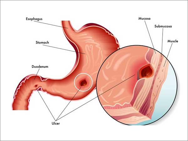
#25 This is Cool » Mount McKinley » 2026-03-31 22:27:55
- Jai Ganesh
- Replies: 0
Denali
Gist
Denali, officially renamed from Mount McKinley in 2015, is the highest mountain peak in North America, reaching a summit elevation of 20,310 feet above sea level. Located in Alaska's Denali National Park and Preserve, this massive granite block is known for extreme, unpredictable weather, and it is considered one of the most challenging, deadly, and scenic climbs in the world.
Mount McKinley is the crown jewel of Denali National Park and Preserve, the highest mountain in North America (at 20,310' above sea level), and a sought-after prize for sightseeing national park visitors and mountain climbing alpinists alike.
Denali, formerly known as Mount McKinley, is the highest mountain peak in North America, towering 20,310 feet above sea level in Alaska's Denali National Park & Preserve. Located in the Alaska Range, it is a premier destination for mountaineering and wilderness exploration, often considered one of the coldest and most challenging mountains in the world.
Summary
Denali, federally designated as Mount McKinley, is the highest mountain peak in North America, with a summit elevation of 20,310 feet (6,190 m) above sea level. It is the tallest mountain in the world from base to peak on land, measuring 18,000 ft (5,500 m). With a topographic prominence of 20,156 feet (6,144 m) and a topographic isolation of 4,621.1 miles (7,436.9 km), Denali is the third most prominent and third-most isolated peak on Earth, after Mount Everest and Aconcagua. Located in the Alaska Range in the interior of the U.S. state of Alaska, Denali is the centerpiece of Denali National Park and Preserve.
The Koyukon people who inhabit the area around the mountain have referred to the peak as "Denali" for centuries. In 1896, a gold prospector named it "Mount McKinley" in support of then–presidential candidate William McKinley, who later became the 25th president; McKinley's name was the official name recognized by the federal government of the United States from 1917 until 2015. In August 2015, 40 years after Alaska had officially named the mountain Denali, the United States Department of the Interior under the Obama administration changed the official federal name of the mountain also to Denali. In January 2025, the Department of the Interior under the Trump administration reverted the mountain's official federal name to Mount McKinley.
In 1903, James Wickersham recorded the first attempt at climbing Denali, which was unsuccessful. In 1906, Frederick Cook claimed the first ascent, but this ascent is unverified and its legitimacy questioned. The first verifiable ascent to Denali's summit was achieved on June 7, 1913, by climbers Hudson Stuck, Harry Karstens, Walter Harper, and Robert Tatum, who went by the South Summit. In 1951, Bradford Washburn pioneered the West Buttress route, considered to be the safest and easiest route, and therefore the most popular currently in use.
On September 2, 2015, the U.S. Geological Survey measured the mountain at 20,310 feet (6,190 m) high, 10 ft lower than the 20,320 feet (6,194 m) measured in 1952 using photogrammetry.
Details
Mount McKinley, highest peak in North America. It is located near the center of the Alaska Range, with two summits rising above the Denali Fault, in south-central Alaska, U.S.
Elevation and geology
Mount McKinley’s official elevation figure of 20,310 feet (6,190 meters), established by the United States Geological Survey in September 2015, was the product of a thorough remeasurement of the mountain’s height conducted earlier that year using state-of-the-art equipment. The new value superseded the long-standing figure of 20,320 feet (6,194 meters) that had been the official elevation since the early 1950s. Earlier attempts to measure the mountain’s height had yielded different values. One such survey, conducted in 2010 using advanced radar technology, was made public in September 2013 and gave its elevation as 20,237 feet (6,168 meters). However, that measurement was subsequently determined to be inaccurate.
Mount McKinley lies about 130 miles (210 km) north-northwest of Anchorage and some 170 miles (275 km) southwest of Fairbanks in Denali National Park and Preserve. The mountain is essentially a giant block of granite that was lifted above Earth’s crust during a period of tectonic activity that began about 60 million years ago. It rises abruptly some 18,000 feet (5,500 meters) from Denali Fault at its base to the higher, more southerly of its two summits. The upper half of the mountain is covered with permanent snowfields that feed many glaciers, some surpassing 30 miles (48 km) in length.
Exploration and climbing attempts
In 1794 the English navigator George Vancouver sighted the mountain from Cook Inlet (an arm of the Gulf of Alaska). The first attempt to climb it was made in 1903 by an American judge, James Wickersham, but it was unsuccessful. A much-publicized but fraudulent claim by the physician and explorer Frederick A. Cook that he had reached the top inspired the conquest of the North Peak in 1910, by two prospectors of what was dubbed the “Sourdough Expedition.” On June 7, 1913, Hudson Stuck and Harry Karstens led a party to the South Peak, the true summit. A climbing party was first airlifted onto the mountain’s flanks in 1932; beginning in the 1950s, that became the standard way to attempt a summit climb, as it reduced the trip by several weeks. Most climbers are now flown to a base camp on southern-facing Kahiltna Glacier at an elevation of 7,200 feet (2,195 meters), where the greatest number follow the West Buttress route. On average, several hundred climbers attempt to reach the summit each year.
Denali or McKinley?
The mountain was known to the Athabaskan Indians as Denali (“The High One” or “The Great One”) and to the Russians as Bolshaya Gora (“Great Mountain”). It was called Densmore’s Mountain in 1889 by Frank Densmore, a prospector. The name Mount McKinley was applied in 1896 by William A. Dickinson, another prospector, in honor of William McKinley (who was elected president of the United States later that year) and became the official name. Efforts began in the mid-1970s to restore the mountain’s original Native American name but faced opposition, mainly from lawmakers from Ohio, McKinley’s home state. However, the mountain’s original name was recognized by the state of Alaska, and it was adopted as the name of the national park and preserve when it was created in 1980.
Use of the name Denali for the mountain became increasingly common, and in 2015 it was officially renamed Denali. On January 20, 2025, as one of his first acts upon his return to the White House, Pres. Donald Trump issued an executive order that called for Denali to be reverted back to Mount McKinley. The following month, the Board on Geographic Names enacted that change. Denali National Park and Preserve retained its current name, however.
Additional Information
Denali (Mount McKinley) is the highest mountain in North America, but controversy surrounds both its height and name.
Denali, also called Mount McKinley, is the tallest mountain in North America, located in south-central Alaska. With a peak that reaches 6,190 meters (20,310 feet) above sea level, Denali is the third-highest of the Seven Summits (the tallest peaks on all seven continents).
Denali is about 210 kilometers (130 miles) north-northwest of Anchorage. Sixty million years ago, tectonic uplift pushed Earth's crust upward, forming Denali and the other Alaska Range mountains. Denali is the centerpiece of the Denali National Park and Preserve, which spans 2.4 million hectares (6 million acres) of land.
“Denali” comes from Koyukon, a traditional Native Alaskan language, and means “the tall one.” This name had been used for many generations and was used by early non-Native researchers and naturalists. But in 1896, William A. Dickinson, a prospector, began calling Denali “Mount McKinley,” in honor of William McKinley, a presidential candidate at the time. After McKinley became president and was later assassinated, Congress formally recognized the name in 1917, despite McKinley’s tenuous ties to Alaska (he had never visited). But Native Alaskans, as well as locals of varied backgrounds, continued to call the mountain Denali. In 1975, a movement began to rename the mountain Denali, but it was blocked by politicians in Ohio, McKinley’s home state. Finally, President Barack Obama and Secretary of the Interior Sally Jewell took action in 2015 to change the name back to Denali, which is now its official name.
In 2015, Denali was measured using state-of-the-art equipment by the United States Geological Survey (USGS), who determined the definitive and now widely accepted height of the mountain: 6,190 meters (20,310 feet). However, a report released in 2013 gave its elevation as 6,168 meters (20,237 feet). Both measurements were different from the long-standing figure of 6,194 meters (20,320 feet) that had been circulated since the 1950s, when the mountain was first measured.
Denali is considered an extremely difficult climb due to the severe weather and steep vertical climbs. In 1906, physician and explorer Frederick Cook was famously reported to have reached the summit, a claim that was later found false. Hudson Stuck, Harry Karstens, and their team of climbers were the first on record to actually reach the summit in 1913. Since then, several hundred people attempt to climb Denali each year.